VML EVK Architecture & Features
Features
-
Renesas RZ/V2L Energy-Efficient Vision-AI MPU
- RZ/V2L Processor Part Number: R9A07G054L23GBG
- 2× Arm Cortex-A55 @ 1.2 GHz
- 1× Arm Cortex-M33 @ 200 MHz
- 1× Arm Mali-G31 3D-GPU @ 500 MHz + Image Scaling Unit
- DRP-AI Accelerator – 1 TOPS/W class; runs Tiny YOLOv2 at 28 fps
- DRP Simple ISP machine-vision library (supports up to 1920×1080)
- H.264 Hardware Video Encode/Decode (1920×1080 @ 30 fps)
- 128 KB ECC on-chip RAM
-
XENO+ VML SOM (R2L100) – 40×40 mm, 176-pin LGA
- 2 GB DDR4-1600 (16-bit single-channel with ECC)
- 8 GB eMMC Flash (upgradeable to 32 GB)
- 16 MB QSPI NOR Boot Flash
- On-module PMIC with 3V3, 1V8, 1V2, 0V8 rails and more
-
VML EVK Carrier Board
- 1 Gbps RGMII Ethernet interfaces (1× RJ45)
- MIPI-DSI display interface – 22-pin FPC + 15-pin FPC connectors
- MIPI-DSI display interface – 22-pin FPC + 15-pin FPC connectors
- MIPI-CSI-2 camera interface – 22-pin FPC + 15-pin FPC connectors
- M.2 connector for Wi-Fi / Bluetooth module
- M.2 connector for LTE module
- SIM card slot (for LTE module)
- 1× USB 2.0 Host interfaces (Type-A) for USB camera
- 2× CAN-FD interfaces
- 5× 12-bit ADC inputs
- 4× I2C interfaces
- 5× UART interfaces
- 2× SPI interfaces
- 2× I2S audio interfaces
- 40-pin expansion header
- 10-pin SWD Programming connector
- JTAG connector
- USB 5V Debug UART interface
- TRRS Audio Jack (stereo output + microphone input)
- Onboard Analog Microphone
- DIP Switches for boot mode selection
- PMIC PWRON button and Reset Switch
- DC Jack 12 V power input
Block Diagram – Renesas RZ/V2L Processor
RZ/V2L Block Diagram
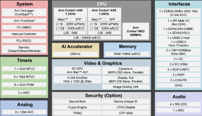
Figure 1: RZ/V2L Processor Block Diagram
The RZ/V2L SoC integrates the following functional subsystems:
| Subsystem | Components / Details |
|---|---|
| CPU Cluster | 2× Arm Cortex-A55 @ 1.2 GHz (L1 I 32KB, L1 D 32KB, L1 D 32KB ECC, L3$ 256KB ECC) |
| Real-Time Core | 1× Arm Cortex-M33 @ 200 MHz + 64 KB on-chip RAM |
| AI Accelerator | DRP-AI: 192 ALU/DMU @ 266 MHz + 576 MAC AI-MAC @ 400 MHz (FP16 data type) |
| 3D Graphics | Arm Mali-G31 GPU |
| Video & Imaging | H.264 Enc/Dec 1920×1080 @ 30fps, ISU, VCP, FCPCS, VCPL4 |
| Camera Input | MIPI CSI-2 (4-lane) + Parallel Input via CRU |
| Display Output | MIPI DSI (4-lane) + Parallel Output via VSPD/DU |
| Memory Interface | DDR3L/DDR4-1600 16-bit with in-line ECC |
| Storage | SDHI/eMMC, SDHI (SD Card), QSPI |
| Connectivity | 2× GbE MAC, 2× USB2.0 (Host + Function), 2× CAN-FD |
| Peripherals | 4× I2C, 5× SCIF (UARTD), 2× SPI/RSPI, 8× 12-bit ADC, 4× SSI (I2S) |
| Security | Secure Boot, Crypto Engine, TRNG, OTP 4Kbit, JTAG Disable |
| System | 16× DMAC, PLL/SSCG, Interrupt Controller, WDT, RTC |
Table 3: Functional subsystems of RZ/V2L Processor
DRP-AI Accelerator Core
The Dynamically Reconfigurable Processor AI (DRP-AI) is a programmable, highly flexible hardware accelerator optimized for vision-AI inference at the edge. It uses FP16 data type, providing higher precision than INT8 used by many competing solutions.
| DRP-AI Resource | Specification | Best Suited For |
|---|---|---|
| DRP | 192 ALU/DMU @ 266 MHz | Pooling, Softmax, activation functions |
| AI-MAC | 576 MAC @ 400 MHz | Convolution operations |
| Data Type | FP16 | Higher precision than INT8 competitors |
| Efficiency | 1 TOPS/W class | Edge AI deployment; Tiny YOLOv2 at 28 fps |
Table 4: DRP-AI Accelerator Specifications
XENO+ VML SOM Block Diagram
The XENO+ VML SOM (R2L100) integrates the RZ/V2L processor with all essential memory, power management, and key interfaces onto a compact 40×40 mm solderable LGA module. The diagram below illustrates SOM internal connectivity.
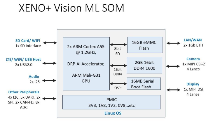
Figure 2: XENO+ R2L100 SOM Block Diagram
| SOM Interface | Connection | External |
|---|---|---|
| 8-bit SD (eMMC) | RZ/V2L SD0/MMC | 16 GB eMMC Flash |
| 16-bit DDR4 | RZ/V2L DDR | 2 GB DDR4-1600 SDRAM |
| QSPI | RZ/V2L QSPI0 | 16 MB Serial NOR Boot Flash |
| SD Interface | RZ/V2L SD1 | Wi-Fi Module or SD Card |
| 2× USB2.0 | RZ/V2L USB | Camera or LTE Module (via EVK) |
| 2× I2S Audio | RZ/V2L SSI | Audio CODEC (via EVK) |
| PMIC | Internal | 3V3, 1V8, 1V2, 0V8 rails |
| 176 LGA Pads | SOM boundary | EVK Carrier Board |
VML EVK Label Diagram
The VML EVK carrier board connects the XENO+ VML SOM to a comprehensive set of peripherals for development and evaluation
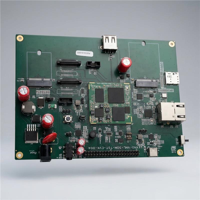
Figure 3: VML EVK Label Diagram
| EVK Interface Block | Description |
|---|---|
| Power Input | 12V DC Barrel Jack → on-board regulation for SOM and peripherals |
| USB 5V DBG UART | USB to SCIF0 - debug console and SCIF download mode |
| PMIC PWRON / Reset | Board power-on and hardware reset buttons |
| DIP Switches | Boot mode selection (BOOT [2:0] configuration) |
| RJ45 Ethernet (×2) | Dual 1 Gbps RGMII Gigabit Ethernet interfaces |
| 40-pin Header | General-purpose expansion connector |
| MIPI-DSI (22+15 FPC) | Dual FPC connectors for display modules |
| MIPI-CSI (22+15 FPC) | Dual FPC connectors for camera modules |
| M.2 Wi-Fi Slot | M.2 connector for Wi-Fi/BT module |
| M.2 LTE Slot | M.2 connector for LTE cellular module |
| SIM Slot | Standard SIM card cage for LTE module |
| USB Type-A (×2) | USB 2.0 Host ports for camera or LTE USB interfaces |
| TRRS Audio Jack | 3.5 mm TRRS stereo output + microphone input |
| Onboard Analog MIC | Built-in microphone for audio capture |
| SWD 10-pin Connector | SWD programming/debug header |
| JTAG Connector | JTAG debug interface |
VML EVK Component Locations
a. Top Side Components
| # | Reference | Description | # | Reference | Description |
|---|---|---|---|---|---|
| 1 | XENO+ SOM | RZ/N2LXENO+ VML SOM (R2L100) | 11 | J_DSI1 | 22-position FPC for DSI display |
| 2 | J_ETH1 | RJ45 1Gbps Ethernet - Port 1 | 12 | J_DSI2 | 15-position FPC for DSI display |
| 3 | J_UART | USB 5V Debug UART connector | 13 | J_CSI1 | 22-position FPC for CSI camera |
| 4 | J_EXP | 40-pin Expansion Header | 14 | J_CSI2 | 15-position FPC for CSI camera |
| 5 | J_AUDIO | TRRS 3.5 mm audio jack | 15 | J_M2_WIFI | M.2 connector for Wi-Fi module |
| 6 | SW_DIP | DIP switches - boot mode selection | 16 | J_M2_LTE | M.2 connector for LTE module |
| 7 | S_PWR | PMIC PWRON button | 17 | J_SIM | SIM card slot |
| 8 | S_RST | Reset switch | 18 | J_USB | USB Type-A host connectors |
| 9 | J_SWD | 10-pin SWD programming connector | 19 | J_JTAG | JTAG debug connector |
| 10 | MK1_AUD | Onboard Analog MIC | 20 | J_DC | 12V DC power input jack |
Table 5: Key Components on VML EVK
Debug Header, Switches and LEDs
A. USB Debug UART Interface
A USB 5V Debug UART interface is provided on the EVK for serial console output and Linux command- line access. Connect a USB cable from the EVK USB DBG UART port to the development computer.
The UART is connected to SCIF0 of the RZ/V2L processor
| Signal | Direction | Description |
|---|---|---|
| TXD | TX → Host | Transmit data from RZ/V2L to host computer |
| RXD | RX ← Host | Receive data from host computer to RZ/V2L |
| GND | – | Signal ground |
UART Settings: 115200 baud, 8N1, no hardware flow control.
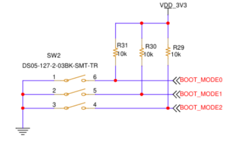
B. DIP Switches and Boot-Mode Selection
The DIP switch bank on the EVK controls the RZ/V2L boot mode by setting the BOOT[2:0] signals. Boot mode is sampled at the end of the hardware reset sequence
| BOOT2 | BOOT1 | BOOT0 | Boot Mode |
|---|---|---|---|
| 0 | 0 | 0 | Boot from SD Card (3V3) |
| 0 | 0 | 1 | Boot from eMMC - 1V8 (Default) |
| 0 | 1 | 1 | Boot from QSPI NOR Flash - 1V8 |
| 1 | 0 | 1 | SCIF Serial Download Mode |
Note:
- BOOT0 is determined by SD card presence
- BOOT Modes are controlled by DIP Switch
C. Push-Button Switches
| Switch | Name | Function |
|---|---|---|
| S_PWR | PMIC PWRON | Board power-on/off control - connected to PMIC PWRON input |
| S_RST | RESET | Hardware reset for RZ/V2L processor and SOM |
D. Status LEDs
| LED | Color | Function |
|---|---|---|
| PWR LED | Green | 3V3 power-good indicator - illuminates when board is powered |
| OC LED | Red | Over-current protection indicator - illuminates when an overcurrent condition is detected on the board power rails |
Memory Resources
The VML EVK provides the following onboard memory resources via the XENO+ VML SOM:
| Memory Type | Interface | Size | Performance | Part Number |
|---|---|---|---|---|
| DDR4 SDRAM | DDR | 2 GB | 1600 MHz, 16-bit bus | Micron MT40A1G16 or equivalent |
| eMMC Flash | SD0 | 8 GB (-32 GB) | 200 MHz, 8-bit bus | Standard eMMC 5.1 device |
| QSPI NOR | QSPI0 | 16 MB | 104 MHz, 4-bit bus | Serial NOR Boot Flash |
| microSD Slot | SD0 | Removable | User-selected card | Determined by user |
A. eMMC Memory (Partition size and Programming)
- For convenience, the procedures for changing partition size and programming new images into eMMC flash memory are included in the Appendix area of this User Guide document
- Configuring and programming the microSD card and QSPI memory use a similar scripted approach, but this is detailed in the software documentation
Peripheral Devices and Interfaces
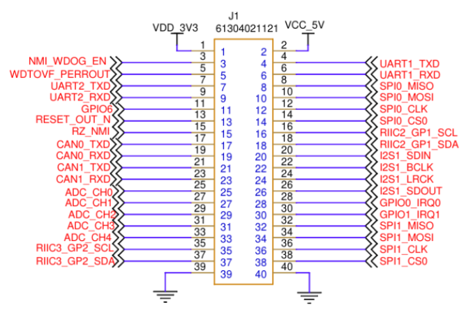
A. 40-Pin Expansion Header
The EVK provides a 40-pin expansion header (2×20 pin, 2.54 mm pitch) exposing GPIO, I2C, SPI, UART, and power rails for interfacing with expansion boards and HAT-compatible add-on modules
| Pin # | Signal | Function | Pin # | Signal | Function |
|---|---|---|---|---|---|
| 1 | VDD_3V3 | 3.3V Power Rail | 2 | VCC_5V | 5V Power Rail |
| 3 | NMI_WDOG_EN | NMI / Watchdog Enable | 4 | UART1_TXD | UART1 Transmit Data |
| 5 | WDTOVF_PERR_OUT | Watchdog Overflow / PERROUT | 6 | UART1_RXD | UART1 Receive Data |
| 7 | UART2_TXD | UART2 Transmit Data | 8 | SPI0_MISO | SPI0 Master-In Slave-Out |
| 9 | UART2_RXD | UART2 Receive Data | 10 | SPI0_MOSI | SPI0 Master-Out Slave-In |
| 11 | GPIO6 | General Purpose I/O | 12 | SPI0_CLK | SPI0 Clock |
| 13 | RESET_OUT_N | System Reset Output (active low) | 14 | SPI0_CS0 | SPI0 Chip Select 0 |
| 15 | RZ_NMI | Non-Maskable Interrupt | 16 | RIIC2_GP1_SCL | I2C Bus 2 - Clock |
| 17 | CAN0_TXD | CAN-FD 0 Transmit | 18 | RIIC2_GP1_SDA | I2C Bus 2 - Data |
| 19 | CAN0_RXD | CAN-FD 0 Receive | 20 | I2S1_SDIN | I2S1 Serial Data In |
| 21 | CAN1_TXD | CAN-FD 1 Transmit | 22 | I2S1_BCLK | I2S1 Bit Clock |
| 23 | CAN1_RXD | CAN-FD 1 Receive | 24 | I2S1_LRCK | I2S1 Left/Right Clock |
| 25 | ADC_CH0 | ADC Channel 0 | 26 | I2S1_SDOUT | I2S1 Serial Data Out |
| 27 | ADC_CH1 | ADC Channel 1 | 28 | GPIO0_IRQ0 | GPIO0 / IRQ Input 0 |
| 29 | ADC_CH2 | ADC Channel 2 | 30 | GPIO1_IRQ1 | GPIO1 / IRQ Input 1 |
| 31 | ADC_CH3 | ADC Channel 3 | 32 | SPI1_MISO | SPI1 Master-In Slave-Out |
| 33 | ADC_CH4 | ADC Channel 4 | 34 | SPI1_MOSI | SPI1 Master-Out Slave-In |
| 35 | RIIC3_GP2_SCL | I2C Bus 3 - Clock | 36 | SPI1_CLK | SPI1 Clock |
| 37 | RIIC3_GP2_SDA | I2C Bus 3 - Data | 38 | SPI1_CS0 | SPI1 Chip Select 0 |
| 39 | GND | Ground | 40 | GND | Ground |
Table 6: 40-Pin Expansion Header Pinout’s
B. SWD / JTAG Debug Interfaces
The EVK provides two debug access paths: a 10-pin SWD programming connector and a dedicated JTAG connector, supporting industry-standard debugger probes.
| Pin | SWD Signal | JTAG Signal | Direction | Description |
|---|---|---|---|---|
| 1 | IF_VREF (1V8) | IF_VREF (1V8) | Input | Target reference voltage for debugger I/O level detection |
| 2 | SWDIO | JTAG_TMS | I/O | SWD data I/O / JTAG Test Mode Select |
| 3 | GND | GND | – | Signal ground |
| 4 | SWCLK | JTAG_TCK | Input | SWD clock / JTAG test clock |
| 5 | GND | GND | – | Signal ground |
| 6 | SWO | JTAG_TDO | Output | SWD trace output / JTAG test data out |
| 7 | N/C | NC | – | Reserved |
| 8 | IF_TDI | JTAG_TDI | Input | Test data input |
| 9 | IF_DETECT | GND | – | Signal ground |
| 10 | IF_RST | JTAG_TRST_N | Input | Target system reset (active low) |
Table 7: SWD/JTAG debugger 10-pin mini-header
C. USB 2.0 Host Interfaces
Two USB 2.0 Type-A host connectors are available on the EVK for connecting USB cameras, LTE USB dongles, or other USB peripheral devices.
| USB Port | Connector | Typical Use |
|---|---|---|
| USB Host 1 | Type-A | USB Camera |
D. MIPI-DSI Display Interface
The EVK provides two FPC connectors for MIPI-DSI display modules, enabling flexibility to connect a wide range of panel types. The 2 & 4 lane MIPI-DSI output from the RZ/V2L is routed to both connectors.
| Connector | Type | Pin Count | Use Case |
|---|---|---|---|
| J_DSI1 | FPC | 22 pins (4 Lane) | Primary DSI display connection |
| J_DSI2 | FPC | 15 pins (2 Lane) | Alternative / secondary DSI display |
E. MIPI-CSI Camera Interface
Two FPC connectors are provided for MIPI-CSI-2 camera modules. The EVK supports 2 MP to 5 MP image sensors in MIPI CSI-2 format at up to 30 fps.
| Connector | Type | Pin Count | Use Case |
|---|---|---|---|
| J_CSI1 | FPC | 22 pins (4 Lane) | Primary CSI camera connection |
| J_CSI2 | FPC | 15 pins (2 Lane) | Alternative / secondary CSI camera |
F. Gigabit Ethernet Interfaces
The EVK features 1 Gbps Gigabit Ethernet ports via RGMII interface, with RJ45 connectors including integrated magnetics, suitable for LAN/WAN connectivity in networking and IoT gateway applications.
| Port | Connector | Interface | Speed |
|---|---|---|---|
| ETH1 | RJ45 with magnetics | RGMII | 10/100/1000 Mbps |
G. M.2 Connectors (Wi-Fi and LTE) Two M.2 expansion slots are provided for wireless connectivity modules.
| Slot | Purpose | Interface | Notes |
|---|---|---|---|
| M.2 Wi-Fi | Wi-Fi / Bluetooth Module | SDIO + UART | Connect to RZ/V2L SD interface |
| M.2 LTE | LTE / 4G Cellular Module | USB 2.0 | Requires SIM card in J_SIM slot |
H. SIM Card Slot
A standard SIM card slot is provided for use with the M.2 LTE module, supporting standard SIM cards for cellular network authentication.
I. CAN-FD Interface
Two CAN-FD interfaces are available on the EVK, routed to the 40-pin expansion header and dedicated connectors, including onboard CAN transceivers for direct bus connection.
| Interface | Signals | Transceiver | Notes |
|---|---|---|---|
| CAN0 | CAN0_TX, CAN0_RX | Onboard | Available on 40-pin header pins |
| CAN1 | CAN1_TX, CAN1_RX | Onboard | Available on 40-pin header pins |
J. ADC Inputs
Five 12-bit ADC channels are available for interfacing with analog sensors, with a 0 V to 1.8 V input range and 1 µs per channel conversion rate.
| ADC Parameter | Value |
|---|---|
| Resolution | 12-bit |
| Input Range | 0 V - 1.8 V |
| Channels | 5 (ADC_CH0 to ADC_CH4) |
| Conversion Rate | 1 µs per channel |
K. Audio Interface
The EVK provides audio capability through a TRRS 3.5 mm audio jack (stereo headphone output + microphone input) and an onboard analog microphone. The audio codec interfaces with the RZ/V2L via I2S (SSI) interface.
| Audio Feature | Description |
|---|---|
| TRRS Audio Jack | 3.5 mm TRRS - stereo left/right output + microphone in |
| Onboard Microphone | Built-in analog microphone for voice/audio capture |
| Interface to SoC | I2S (SSI) - 2× I2S audio interfaces |
| Audio Codec | External codec IC on EVK carrier board |
Wireless Connectivity
A. Wi-Fi / Bluetooth (M.2 Module)
Wi-Fi and Bluetooth connectivity is provided via an M.2 module installed in the dedicated M.2 Wi-Fi slot. The module interfaces with the RZ/V2L via SDIO for Wi-Fi data and UART for Bluetooth control.
| Interface | Signal | Protocol |
|---|---|---|
| Wi-Fi Data | RZ_SD1 (4-bit SDIO) | SDIO 3.0 |
| BT Control | RZ_SCIF3 (4-wire UART) | UART with hardware flow control |
B. LTE / 4G Cellular (M.2 Module) LTE connectivity is supported via an M.2 LTE module installed in the dedicated LTE M.2 slot
The module connects over USB 2.0 and requires a SIM card inserted in the onboard SIM slot.
| Interface | Signal | Notes |
|---|---|---|
| LTE Data | USB 2.0 | Via onboard USB Host interface |
| SIM Card | SIM Slot | Standard SIM card, 1.8V / 3V |
Power Architecture
A. Power Input
The VML EVK is powered via a DC barrel jack accepting 12 V input. The onboard power regulation circuitry converts the 12 V input to all required voltage rails for the XENO+ VML SOM and EVK peripherals. A minimum 2 A supply is recommended; 3 A or higher is advised when M.2 modules are fitted
| Power Input | Connector | Voltage | Recommended Rating |
|---|---|---|---|
| Main Power | DC Barrel Jack | 12 V DC | ≥ 2 A (3 A recommended with modules) |
B. Power Regulation
The XENO+ VML SOM integrates a Renesas PMIC (Power Management IC) that efficiently distributes power to all SoC subsystems. The EVK carrier adds additional regulation for peripheral circuits.
| Rail | Voltage | Powers |
|---|---|---|
| VDD_1V1 | 1.1 V | RZ/V2L core VDD and PLLs |
| VDDQ_1V2 | 1.2 V | DDR4 VDDQ |
| VDD_1V8 | 1.8 V | I/O, ADC, eMMC, QSPI, USB, Wi-Fi/BT, level shifters |
| VDD_3V3 | 3.3 V | Ethernet PHY, USB Hub, CSI, DSI, CAN, Expansion Header |
| VDD_0V8 | 0.8 V | RZ/V2L internal power rails |
| SD_PVDD | 3.3V / 1.8V switchable | SD Card / eMMC interface |
C. Power Consumption
The VML EVK with XENO+ SOM is a power-efficient platform. Typical power consumption ranges from approximately 2 W (idle) to 6 W (full AI inference load), depending on active peripherals and workload. Connecting M.2 Wi-Fi or LTE modules will increase power consumption.
| Operating Mode | Typical Power |
|---|---|
| Idle / Standby | ~1.5 - 2.5 W |
| Linux Active (no AI) | ~2.5 - 3.5 W |
| DRP-AI Inference Active | ~4.0 - 6.0 W |
| With Wi-Fi + LTE Active | Add ~1.5 - 2.5 W |
ESD Protection
All USB interfaces and the Ethernet interfaces on the EVK include high-speed ESD protection devices on both power rails and data lines. The CAN interfaces also include ESD protection transient voltage suppressors. Handle the board carefully and follow standard ESD precautions.